Nanoimprint Lithography: Stop Saying It Will Replace EUV
Every 6 months or so, we see another round of headlines about nanoimprint lithography disrupting EUV.
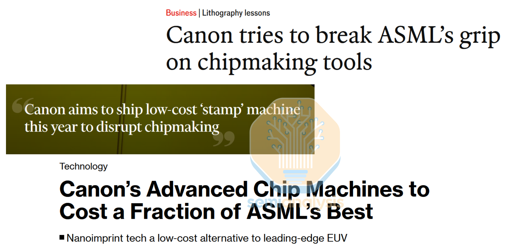
It makes for good clickbait but is just not true. The technology has many interesting and valid applications, but nothing like what EUV can do. Theoretically, NIL could match or even exceed EUV capabilities. Practically, there are serious issues for NIL without any clear way forward.
We’ll explain those differences in theory versus actual in-fab practice in this report. We’ll also detail the key players in the market and the likely applications where it will work. To start, let’s cover the basics of what NIL is and what it can do:
NIL Basics & History
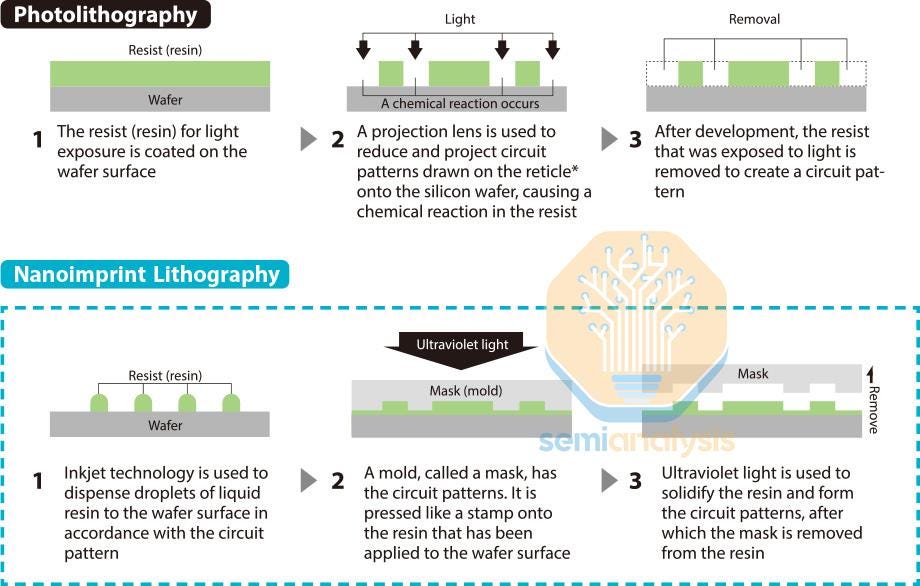
Nanoimprint lithography uses a patterned “stamp” to imprint a pattern in resin. In semiconductor production, it achieves the same end goal as photolithography à la ASML – transfer a pattern from a mask onto a wafer. These patterns are just 1 layer of the chip design. Stacking 50-100 layers, with patterning followed by other techniques like etch and deposition on each, eventually builds up a complete chip.
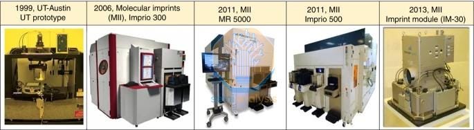
The most promising technique for nanometer-scale NIL was invented in 1996 and spun out from academia to a commercial entity in 2001 as Molecular Imprints Inc. (MII). Canon acquired MII in 2014, positioning it as their alternative at the time ASML was beginning to ship EUV into customer R&D fabs.
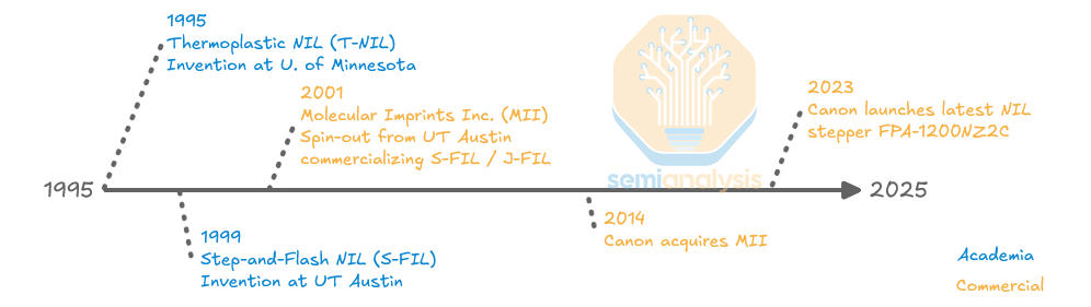
This is the only advanced commercial venture into NIL technology. A Chinese competitor, Prinano, recently made headlines, but is much less mature, for now. Nanonex, spun out by the inventors of NIL from the University of Minnesota, has fewer than 100 tools worldwide, mostly in academic labs. EV Group has commercial tools but explicitly aims for less advanced applications including metalenses, MEMS, and microfluidics.
Canon went all-in on NIL as its next-gen patterning tech after DUV. It’s the only thing on their roadmap beyond KrF scanners, which were state-of-the-art in 2000. As we’ll see, it was the wrong bet.
Detailed Process Flow
Canon calls its technology “J-FIL” for jet and flash and nanoimprint lithography. “Jet” refers to the method of applying resist to the wafer, followed by imprinting by the template and a “flash” of UV light to cure the resist in place.
Producing an NIL imprint starts with dispensing photoresist on
...This excerpt is provided for preview purposes. Full article content is available on the original publication.