How ASML Got EUV
Deep Dives
Explore related topics with these Wikipedia articles, rewritten for enjoyable reading:
-
Moore's law
13 min read
Linked in the article (27 min read)
-
7 nm process
12 min read
Linked in the article (14 min read)
-
Plasma etching
11 min read
Linked in the article (7 min read)
I am pleased to cross-post this piece with Factory Settings, the new Substack from IFP. Factory Settings will feature essays from the inaugural CHIPS team about why CHIPS succeeded, where it stumbled, and its lessons for state capacity and industrial policy. You can subscribe here.
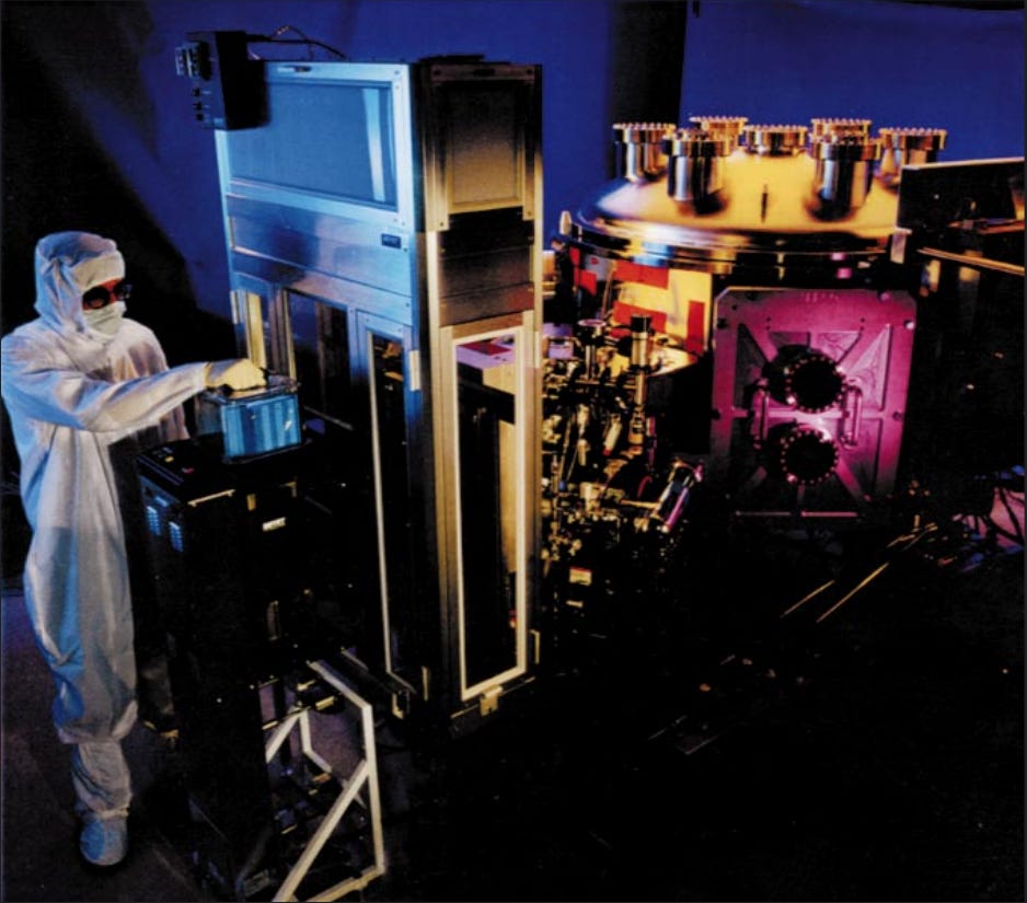
Moore’s Law, the observation that the number of transistors on an integrated circuit tends to double every two years, has progressed in large part thanks to advances in lithography: techniques for creating microscopic patterns on silicon wafers. The steadily shrinking size of transistors — from around 10,000 nanometers in the early 1970s to around 20-60 nanometers today — has been made possible by developing lithography methods capable of patterning smaller and smaller features.1 The most recent advance in lithography is the adoption of Extreme Ultraviolet (EUV) lithography, which uses light at a wavelength of 13.5 nanometers to create patterns on chips.
EUV lithography machines are famously made by just a single firm, ASML in the Netherlands, and determining who has access to the machines has become a major geopolitical concern. However, though they’re built by ASML, much of the research that made the machines possible was done in the US. Some of the most storied names in US research and development — DARPA, Bell Labs, IBM Research, Intel, the US National Laboratories — spent decades of research and hundreds of millions of dollars to make EUV possible.
So why, after all that effort by the US, did EUV end up being commercialized by a single firm in the Netherlands?
How semiconductor lithography works
Briefly, semiconductor lithography works by selectively projecting light onto a silicon wafer using a mask. When light shines through the mask (or reflects off the mask in EUV), the patterns on that mask are projected onto the silicon wafer, which is covered with a chemical called photoresist. When the light strikes the photoresist, it either hardens or softens the photoresist (depending on the type). The wafer is then washed, removing any softened photoresist and leaving behind hardened photoresist in the pattern that needs to be applied. The wafer will then be exposed to a corrosive chemical, typically plasma, removing material from the wafer in the places where the photoresist has been washed away. The remaining hardened photoresist is then removed, leaving only an etched pattern in
...This excerpt is provided for preview purposes. Full article content is available on the original publication.