How Far Can Chinese HBM Go?
Deep Dives
Explore related topics with these Wikipedia articles, rewritten for enjoyable reading:
-
High Bandwidth Memory
9 min read
The article centers on HBM technology but assumes reader familiarity with its technical architecture. Wikipedia's article explains the stacking technology, TSV interconnects, and generational differences (HBM, HBM2, HBM3) that would deepen understanding of why this is such a difficult manufacturing challenge.
-
Extreme ultraviolet lithography
13 min read
The article identifies EUV as the critical chokepoint preventing China from advancing beyond certain DRAM nodes. Understanding the physics of EUV, why ASML has a monopoly, and the decades of development required would illuminate why this export control is so effective.
-
Dynamic random-access memory
12 min read
The article discusses DRAM manufacturing nodes, capacitor structures, and wordlines/bitlines without explaining how DRAM fundamentally works. Understanding the one-transistor one-capacitor cell structure and refresh requirements would help readers grasp why scaling is so challenging.
This December, we’re teaming up with GiveDirectly to send cash to 800 impoverished families in the Bikara region of Rwanda. Studies show that direct cash transfers have a multiplier effect of 2.5x in local economies and reduce infant mortality rates by 48%. Your donation is also tax-deductible in the United States. The link to give is here, and the deadline for donations is midnight on December 31st. Please consider donating if you can!
is a researcher focused on semiconductors, AI, China, and Taiwan. He holds a Master’s degree in Regional Studies — East Asia from Harvard and was recently a summer fellow at the Centre for the Governance of AI (GovAI).
High-bandwidth memory, or HBM, remains the key bottleneck for China to catch up in manufacturing advanced AI chips. As Moore’s Law has more or less held steady, logic nodes have continuously progressed.
However, the rate of memory chip progression has been slow compared to logic chips. Thus, AI operations are often “memory constrained,” meaning that compute is sitting idle waiting for the memory chip to feed it data on which to perform operations. HBM was created to address this “memory wall” by stacking multiple memory chips on top of each other to boost memory bandwidth. As AI chips continue to get better, HBM remains a critical component for scaling. Simply put, if you care about the AI race and AI chips, then you must care about HBM.
Although China’s memory champion CXMT has been closing the HBM gap, the three memory giants of SK Hynix, Samsung, and Micron continue to be more than two generations ahead of CXMT’s HBM2. Assuming export controls hold steady, China’s HBM advances will continue to be stymied by a lack of advanced equipment.
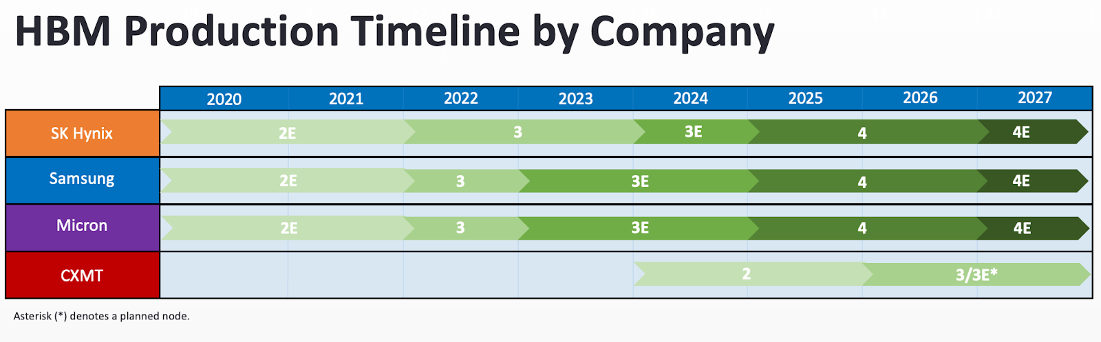
For perspective, achieving the industry’s current HBM3E and HBM4 would be a tremendous achievement for China. As of November 2025, the most advanced AI chips in use use HBM3E. H100s, B100s, and other leading GPUs tap into HBM3E for memory, while Nvidia’s upcoming Rubin GPUs will use HBM4. If CXMT can achieve HBM4 quickly, then they will be able to crack a key part of making advanced GPUs. However, even if they are able to make HBM4 several years down the line, competitive AI chips will likely have meteored beyond contemporary standards to handle workloads unimaginable today.
Ray Wang’s piece earlier this year
...This excerpt is provided for preview purposes. Full article content is available on the original publication.