How to Kill 2 Monopolies with 1 Tool
Deep Dives
Explore related topics with these Wikipedia articles, rewritten for enjoyable reading:
-
Extreme ultraviolet lithography
13 min read
The article extensively discusses EUV lithography as the current industry standard that Substrate's X-ray lithography aims to disrupt. Understanding EUV's technical foundations, challenges, and ASML's monopoly provides essential context for evaluating the significance of Substrate's claims.
-
Synchrotron light source
14 min read
The article mentions that Substrate's approach may use a large synchrotron or particle accelerator to generate sub-EUV wavelengths. Understanding how synchrotrons produce intense X-ray beams and their historical role in semiconductor research illuminates why this technology could enable a breakthrough in lithography.
-
Multiple patterning
14 min read
The article repeatedly references multi-patterning as a key cost driver and complexity factor in current semiconductor manufacturing that Substrate's single-patterning X-ray approach could eliminate. Understanding why multiple exposures became necessary and their economic impact clarifies why single-patterning at advanced nodes would be revolutionary.
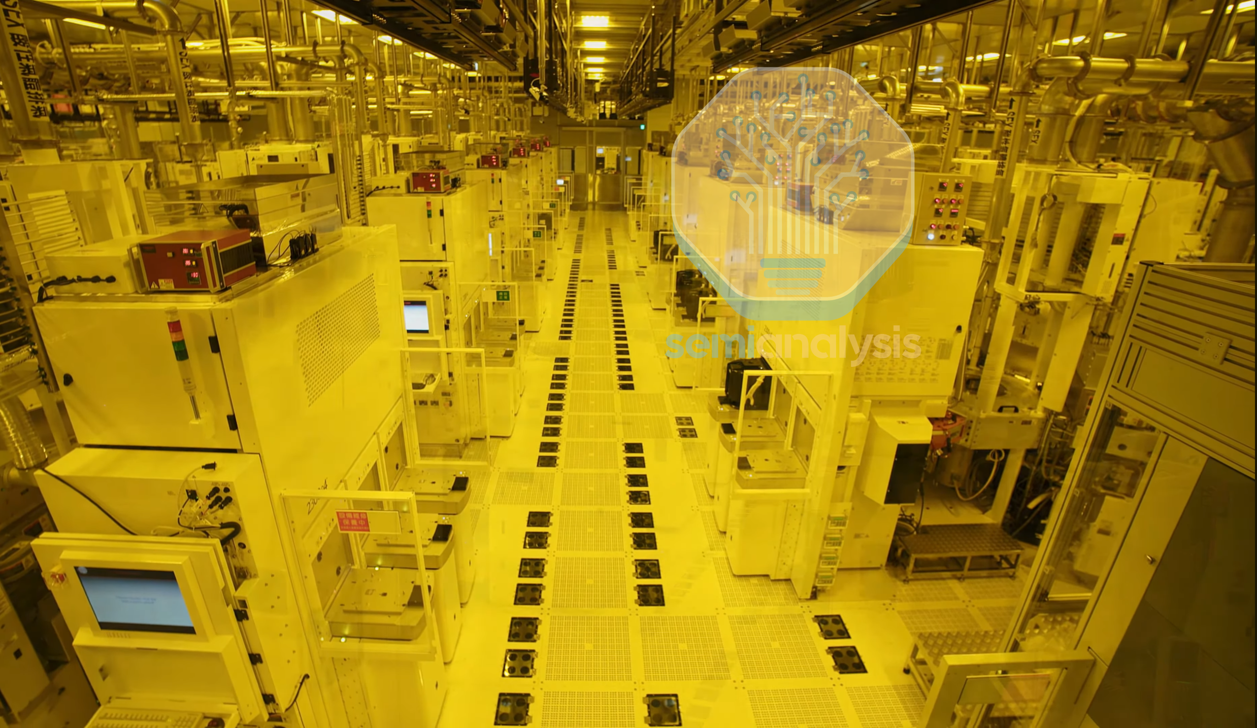
The chipmaking industry is, surprisingly, ripe for disruption. Technical decisions at incumbents are often driven by inertia, “that’s what we’ve always done.” Regression is feared above all else. Something as simple as fab lighting color cannot be changed: traditional yellow lights are still used in photolithography lines even though fabs will readily tell you it no longer has any risk of affecting the photoresist.
This has worsened in recent years. Chipmakers iterate on existing technology despite slower scaling and rapidly increasing costs. ASML has a tool on their roadmap, hyper-NA, that they openly admit may not be economically viable! But it’s hard to fault these companies – the tools and fabs print a lot of money. A single EUV tool, sold for $225M, can produce more than $650M in complete wafers in a year (note that there are many costs beyond that single EUV tool incurred in producing those wafers). There is little incentive for incumbents to change tack.
But that leaves an opening for masochistic bold, scrappy innovators… enter Substrate.
X-Ray Lithography
Substrate is a recently out-of-stealth Bay Area startup inventing “technology to power next-generation foundries” with the mission to substantially reduce the cost of advanced logic wafers. The first major step towards this mission is a new X-ray lithography (XRL) tool that the company has invented.
The idea of x-ray lithography has been around for half a century. MIT researchers produced the first functioning devices using XRL in 1972. Most labs doing lithography research at least experimented with it - Bell Labs, IBM, and others. IBM even built chips using XRL in the 90s, but long wavelength (DUV and above) techniques kept scaling, so there was no need to overcome the numerous challenges facing XRL. Chief among them are (a) optics, since just like EUV, almost nothing bends nor reflects X-ray wavelengths and (b) sources, since generating a bright, isochromatic, and stable source of soft X-rays typically requires massive particle accelerators.
The fields of spectroscopy and microscopy continued ahead with soft x-ray technology even after chip industry interest moved elsewhere. High quality research-grade optics and ‘tabletop’-scale sources have been a focus of intense research, but nothing resembling a leading edge lithography system has gone public.
It appears Substrate has overcome these x-ray challenges at least partially, and their performance claims are stunning:
Single-patterning
This excerpt is provided for preview purposes. Full article content is available on the original publication.