Why Faster PHY Design is the Low-Hanging Fruit in Custom HBM4 Base Die
Welcome to a 🔒 subscriber-only deep-dive edition 🔒 of my weekly newsletter. Each week, I help investors, professionals and students stay up-to-date on complex topics, and navigate the semiconductor industry.
If you’re new, start here. As a paid subscriber, you will get additional in-depth content. We also have student discounts and lower pricing for purchasing power parity (see discounts). See here for all the benefits of upgrading your subscription tier!
I’ve written a lot of articles on memory recently: why high bandwidth memory is so difficult to make, the case for high bandwidth flash, the packaging challenges involved, why memory is so important, and why there is an impending memory supercycle of which HBM is an integral part.
One important aspect that requires a detailed look is the base die that sits under the stack of DRAM die in HBM. This die is usually slightly larger than the DRAM chips stacked on top and ensures communication between the XPU and DRAM stack. From HBM4 onwards, the base die is going to get increasingly customized because its current implementation leaves a lot on the table in terms of performance, power and functionality.
In this post, we will look at why improved PHY design is the easiest upgrade possible using custom base dies designed for HBM4. In case you’re not familiar with the term, PHY is an abstraction in the Open Systems Interconnect (OSI) networking model for the physical layer where bits are transported from one point to another.
For free subscribers:
Basic Structure of DRAM Memory in HBM: How memory is addressed in HBM memory
Functions of HBM Base Die: The primary functions of HBM base die, and why PHY interconnect is a key element.
For paid subscribers:
Marvell and Eliyan: Benefits of using truly high-speed PHY built in advanced logic nodes, especially those designed at the 3nm node as demonstrated by Marvell and Eliyan.
UCIe: The option to use UCIe in HBM base die by licensing IP from Cadence/Synopsys.
Custom designs and key performance trends: Proprietary base die design from Nvidia/AMD, and latest trends in emerging die-to-die interconnect technology.
Read Time: 12 min
Basic Structure of DRAM Memory in HBM
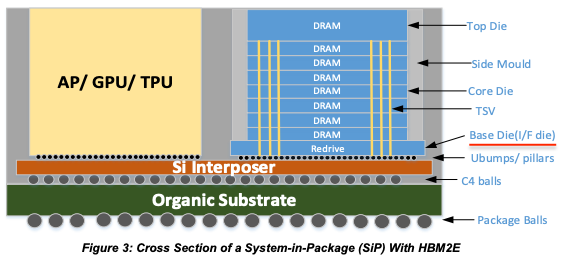
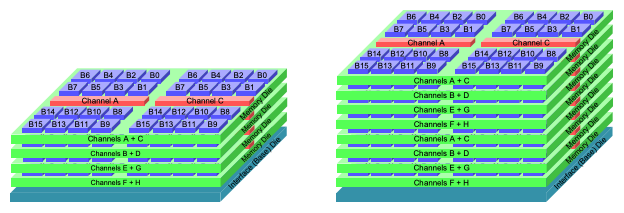
First, let’s look at a basic example of how memory is accessed in HBM. The figure below shows HBM2e with 4- and 8-high stacks of DRAM.
This excerpt is provided for preview purposes. Full article content is available on the original publication.