Intel 18A Details & Cost, Future of DRAM 4F2 vs 3D, Backside Power Adoption (or Not), China's FlipFET, Digital Twins from Atoms to Fabs, and More
Long time readers will recall that SemiAnalysis covers more than just datacenters and AMD. Today we’re back to semiconductors with a tech-focused roundup of the best from this year’s VLSI conference, the premiere design and integration. That includes the latest in chips manufacturing: fab digital twins, the future of advanced logic transistors and interconnects, DRAM architectures beyond the 1x nm nodes, and more. We’ll discuss Intel’s 18A process and compare with TSMC, where backside power will be adopted (and where it won’t), and the likely winners in 4F2 versus 3D DRAM.
Digital Twins: From Atoms to Fabs
Semiconductor design and fabrication is getting exponentially more complex, increasing development costs and lengthening design cycles. Digital twins allow for design exploration and optimization to be done in an accelerated virtual environment. With this, engineers can ensure that designs work before any silicon is run through the fab.
Digital twins span the entire scale of semiconductor design:
Atomic-level: Simulate the quantum and Newtonian interactions between atoms in materials engineering of transistor contacts and gates
Wafer-level: Optimize tool chambers and process recipes in virtual silicon for yield and performance
Fab-level: Maximize fab productivity with orchestrated maintenance and management across the fleet
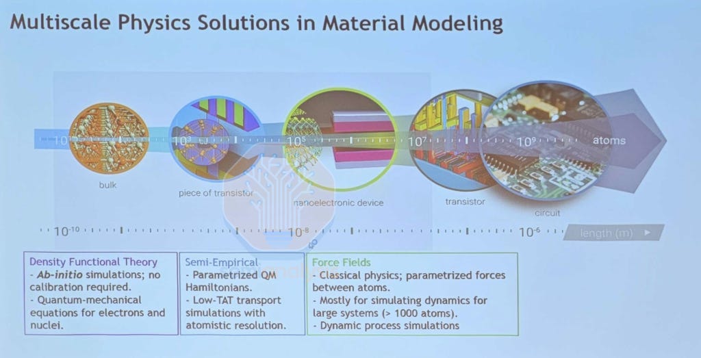
On atomistic simulations, Synopsys provided an overview of their QuantumATK suite, used in materials engineering in transistor contacts and gate oxide stack design, which are critical to device performance. Traditional Density Functional Theory (DFT) modelling of quantum effects between atoms is the most accurate but computationally expensive, while conventional force field simulation of Newtonian atomic interactions is quick but with limited accuracy. GPU accelerated DFT-NEGF (Non-Equilibrium Green’s Function) demonstrated a 9.3x speedup using only 4x A100 vs CPU, while Machine-Learned Force Field simulation using Moment Tensor Potentials demonstrated near-DFT accuracy with 17 min compute cost vs 12 days with traditional DFT.
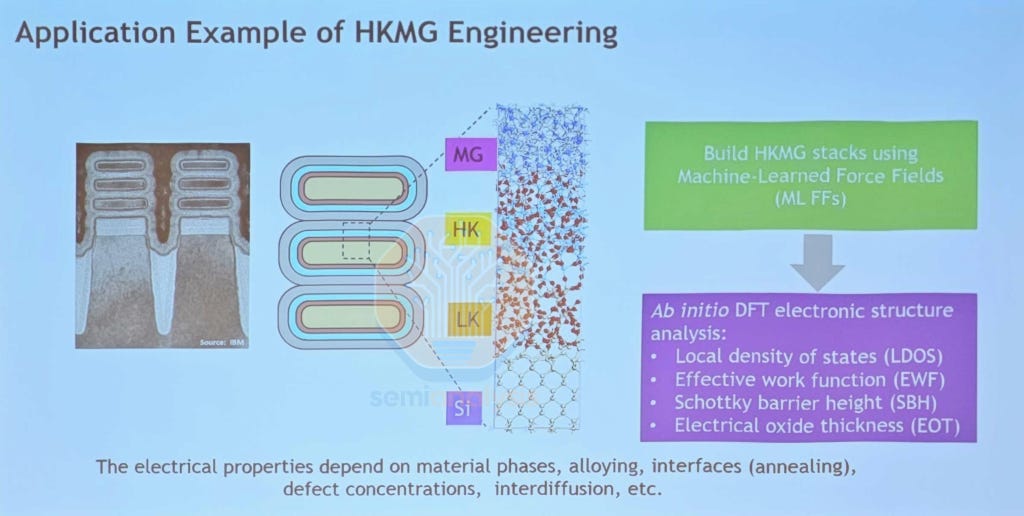
These atomic models are critical in understanding the electrical interactions occurring at the interface between different material layers. In contact engineering, MLFF is used to generate the contact interface between crystalline silicon and amorphous silicides, simulating the depth of interdiffusion where the boundary undergoes silicidation. DFT-NEGF is then used to calculate contact resistance and current-voltage curves across the interface. For gate oxide design, the complex multi-layer work function metal stack is built using MLFF and simulated to check its structure and chemical composition. Dipole dopants can then be introduced and optimized with DFT, which also does electrostatic
...This excerpt is provided for preview purposes. Full article content is available on the original publication.