An In-Depth Look at the Viability of X-rays as an Alternative to EUV Lithography
Deep Dives
Explore related topics with these Wikipedia articles, rewritten for enjoyable reading:
-
LIGA
1 min read
Linked in the article (9 min read)
-
Extreme ultraviolet lithography
13 min read
The article extensively discusses EUV as the current leading-edge technology that X-ray lithography aims to succeed. Understanding EUV's technical foundations, development history, and current limitations would provide essential context for evaluating Substrate's X-ray alternative.
-
Photolithography
13 min read
The article traces the evolution of lithography from Jay Lathrop's inverted microscope through DUV to immersion lithography. A deep understanding of the physics behind photolithography—including the Rayleigh criterion, numerical aperture, and wavelength constraints—is foundational to understanding why X-ray lithography is being explored as the next frontier.
Welcome to a 🔒 subscriber-only deep-dive edition 🔒 of my weekly newsletter. Each week, I help investors, professionals and students stay up-to-date on complex topics, and navigate the semiconductor industry.
If you’re new, start here. See here for all the benefits of upgrading your subscription tier!
As a paid subscriber, you also have access to a video explanation of this post, an executive summary with key highlights, and a google drive link to this article so that you can parse it with your favorite LLM to mine insights best suited to your needs.
On October 28th 2025, Substrate emerged from stealth with $100M in funding and a $1B valuation. The California startup has demonstrated proof-of-concept lithography tools competitive with ASML and fabs like TSMC, Intel and Samsung capable of leading edge nodes at potentially a fraction of the cost. The specific interest centers on X-ray lithography (XRL) as a successor to extreme ultraviolet (EUV) lithography used in today’s leading chip technologies.
This matters because TSMC, Samsung, and hopefully Intel, are the only foundries capable of mass-producing chips at the leading edge and ASML is the sole provider of lithography tools capable of producing these advanced nodes. Already, most American major fabless companies heavily rely on TSMC to manufacture their chips. Substrate’s technology might change all that. America once led chip manufacturing but ceded that position to Taiwan over decades of policy decisions. Substrate’s success means that America “will lead again” in chip manufacturing — if the technology actually pans out at scale.
To be clear, I actually have no idea if this will work, if Substrate’s claims are actually true, or how skeptical one has to be. Take any drastic claims with a healthy grain of salt, because, as Substrate’s CEO James Proud has said himself, this is an incredibly difficult problem but an extremely important one.
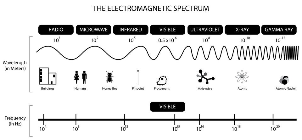
This article is intended to provide a better understanding of XRL as a logical successor to EUV. To provide context, we will start with the basics of lithography and trace its evolution so that the need for XRL is clear. Then, we will discuss the challenges and benefits of XRL, and conclude with some thoughts on Substrate.
Here is an outline:
Photolithography and optical masks
Wavelength and Aperture for photolithography
EUV lithography
X-ray lithography and Substrate
X-ray sources
Challenges in X-ray
This excerpt is provided for preview purposes. Full article content is available on the original publication.